Vexon-1
● FPGA-VERIFIED
Technical profile of Vexon-1, German semiconductor IP: architecture, key figures and verification status — measured on two FPGA platforms.
What Vexon-1 is
Vexon-1 is a specialized compute core for the math of modern language models — matrix multiplication, attention, accumulation. Multi-tile compute with hardware attention and on-chip KV-Cache.
Unlike general-purpose GPUs, Vexon-1 is built for one task: transformer inference on the device. That keeps the block small and efficient — and makes it licensable IP for applications where data must not leave the device.
Explore Vexon-1
A simplified 3D model of the chip design: rotate it, pull it apart and select a layer to see what it does.
Drag to rotate · tap a layer or use Tab and the arrow keys
Three tiles compute at the same time – up to three are validated in parallel in hardware today. Stylized: data reaches the tiles via AXI4 and the on-chip bus; the RISC-V core controls the sequence.
Select a layer to learn more.
Documents
Data sheet, design and test specification: on request under NDA. Request data sheet →
Specification
The five core innovations
Each innovation measurable in hardware — reproducible via REST API on the FPGA prototype.
Sparse Engine
Detects null inputs in language models and skips the multiplication. Less power, less latency, same math.
Adaptive Precision
Automatically switches precision adaptively when data allows — up to 4× more throughput per cycle.
Multi-Tile
Multiple compute units work in parallel — parallel throughput instead of sequential computation.
Hardware Attention
The Transformer core as a dedicated state machine in hardware — including softmax and zero-score filter.
On-chip KV-Cache
The language model memory lives directly on the chip instead of slow external memory. No cloud, no DRAM round-trip.
Verification status
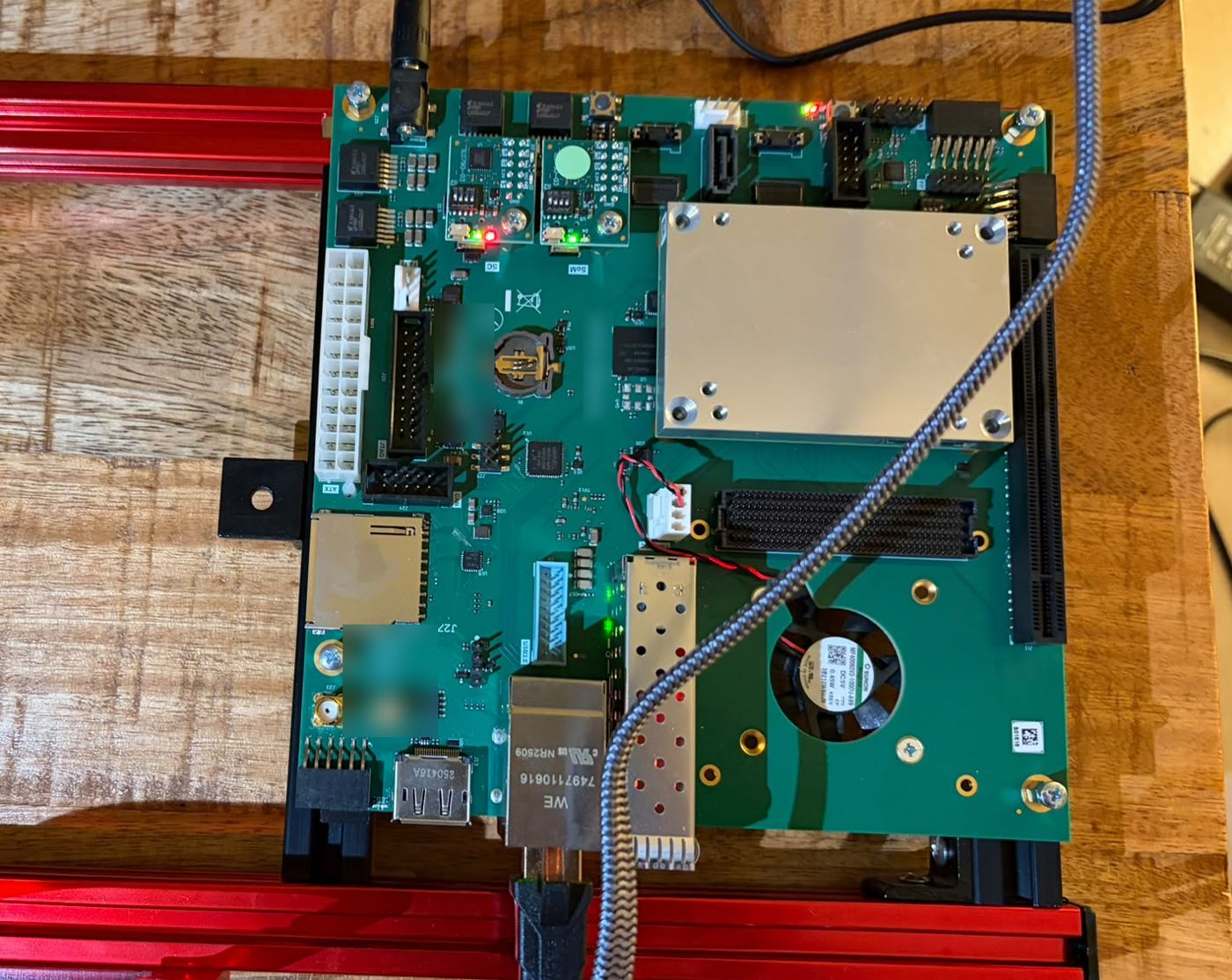
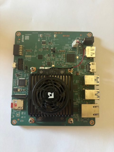
Vexon-1 runs today on two FPGA platforms: the AMD Kria KV260 and a larger Zynq UltraScale+ device (ZU15EG). All five core innovations are proven in hardware through the real DMA driver path — bit-exact against the reference model, with one 32×32 tile or up to three 16×16 tiles in parallel. Measurements are taken directly on the target system, with no host PC in the data path.
In simulation, 14 parametric testbenches with more than 10,000 automated test cases check every configuration bit-exact against a reference model. Code coverage over the core RTL is 92%. As system context, the NPU computes a typical matrix multiplication end to end 4.6× faster than all four CPU cores of the same chip combined; this is a reference point, not a comparison with other NPU IP. The verification pipeline is the foundation for the ASIC stage.
2
FPGA platforms
3
tiles in parallel, bit-exact
92%
code coverage, core RTL
10,000+
test cases in 14 testbenches
Just the beginning
Vexon-1 is verified today as an FPGA prototype — connected via a standard AXI4 interface, as is common in the chip industry. This makes the NPU block cleanly integrable into third-party SoC designs.
The modular multi-tile architecture is built to scale: up to three tiles compute in parallel on the FPGA today, each bit-exact, and the tile count is an RTL parameter. The next steps are larger arrays in the ASIC and chiplet approaches.
Scaling path — verified today, the further stages are target and concept.
See Vexon-1 in action
Demo, technical specification or an architecture discussion — we take the time.